


Kutztown University Scanning Electron Microscope Lab
A powerful tool for discovering nature's wonders
The Fred and Martha Hafer Scanning Electron Microscope Lab at Kutztown University of Pennsylvania is a place where undergraduate students and faculty perform cutting-edge research and explore our world on a micro- and nano-scale.
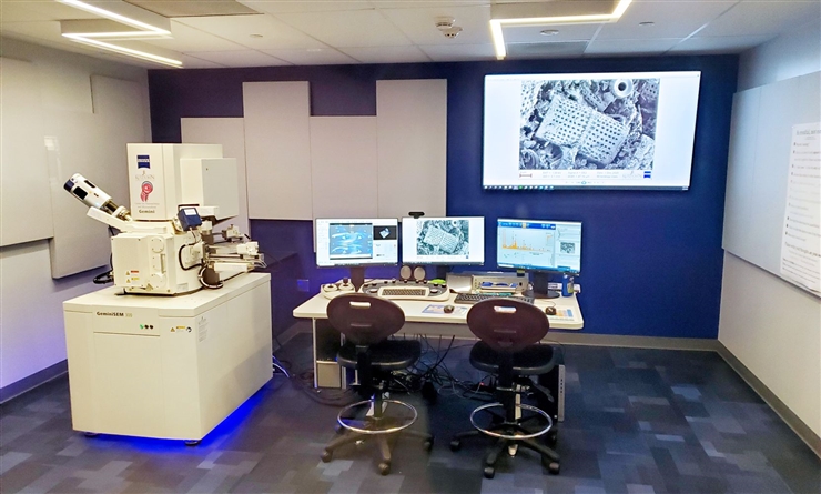
Our Zeiss Gemini 300 Field Emission Scanning Electron Microscope (FE-SEM), is a powerful instrument that uses a perfectly straight lightning bolt (electrons) one third of the width of a human hair to see extremely small things.
We can digitally photograph things as small as 20 nanometers wide. For comparison, a single grain of salt is 300,000 nanometers wide!
Our “resolution limit” detects gaps between things 0.8 nanometers apart.
Who uses the lab?
Our electron microscope is used mostly by Kutztown undergraduate science and art students to study dinosaur eggs, pathogenic fungi, insect anatomy, archeological artifacts, growth of polymers and engineered nanoparticles, formation of crystals in ceramic glazes, and the origin of gold deposits in the Earth.
Does the lab collaborate with others?
YES! We like to collaborate with middle- and high school classes. Students from regional schools provide their own samples that they collected to answer some scientific question they are asking. Classes can either visit the lab in person, or they can analyze their samples from their own classrooms by controlling the SEM remotely.
Because we believe in community, we also collaborate on projects with students from other universities and with local industry who lack electron microscopy facilities.
What can we See with the electron microscope?
Our microscope has many types of electron detectors, each of which sees things in different ways:
-
Everhart-Thornley Secondary Electron Detector = great for seeing 3-D shapes of tiny surfaces
Everhart-Thornley Secondary Electron Detector = great for seeing 3-D shapes of tiny surfaces
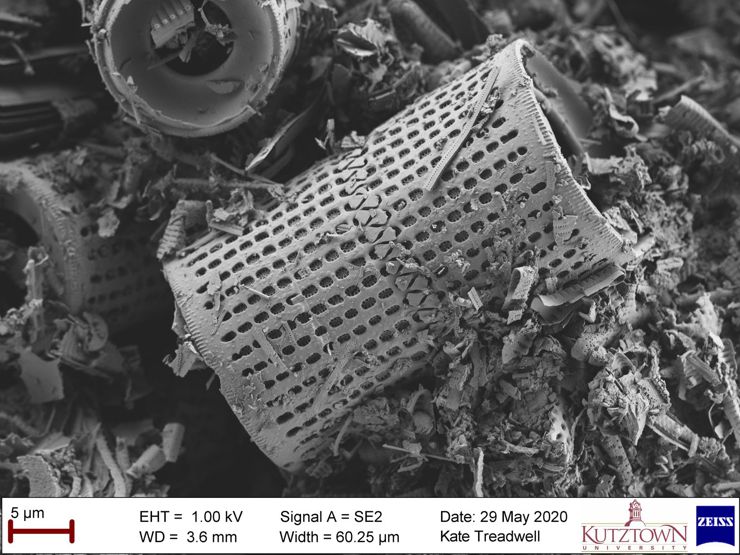
This is the typical detector that’s on almost every SEM. Because it is mounted on the side of the sample chamber, these photos have a shaded appearance that looks 3-dimensional. This low magnification image of a single diatom (plankton) was taken by student Kate Treadwell using the Everhart-Thornley Secondary Electron Detector (SE2). The shell is made of hard quartz to protect the organism, and the pores on the sides enable the diatom to bring CO2 and H2O into the cell for photosynthesis. Plankton like this are responsible for producing half of the oxygen in our atmosphere. Every second breath we take came from the ocean!
-
In-lens Secondary Electron Detector = best for extremely small (nanometer-scale) imaging
In-lens Secondary Electron Detector = best for extremely small (nanometer-scale) imaging
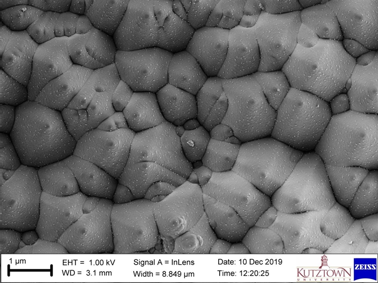
This is a specialty detector that is located directly above the sample. It uses the electric field in the column to amplify the signal coming from the sample. An amplified signal enables us to see EXTRA small things. This image of a solar energy cell surface was taken using the In-lens Secondary Electron Detector (in-lens) by Kutztown University physics professor Dr. Justin Smoyer. The surface feels smooth to the touch, but is actually covered with millions of tiny crystal peaks, and each peak is itself covered by tinier crystals (white dots).
-
Variable Pressure Secondary Electron Detector = for analyzing shapes of nonconductive samples without coating
Variable Pressure Secondary Electron Detector = for analyzing shapes of nonconductive samples without coating
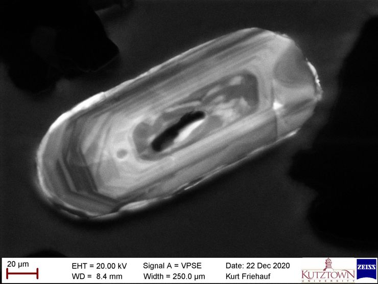
When samples are electrical insulators, the electron beam can build up a static electric charge on the surface (like when you rub a balloon on your head). That static electric charge buildup causes two problems. 1) The charged spot deflects the electron beam, which causes distortions in the image. 2) The charged spot randomly shoots electrons to the detectors, creating a staticy in the image (noise). We can prevent static electric charge from building up by pfffffting a little nitrogen gas onto the sample surface. The Variable Pressure Secondary Electron Detector (VPSE) is designed to “see through that gas" to take pictures of tiny electrically-insulating samples. We also use the VPSE detector for cathodoluminescence imaging to see trace element variations that glow differently under the electron beam. This image of growth zones in a zircon crystal. When crystals form in hot lava, the grown in concentric rings - it's sort of analogous to tree rings. When each new crystal layer forms as molten lava crystallize, trace compositional differences get incorporated into the layer which can cause the sample to “glow” differently (image by Kurt Friehauf). Each bright band formed as the crystal grew episodically.
-
Backscatter Electron Detector (in chamber) = highlights differences between grains with different chemical compositions
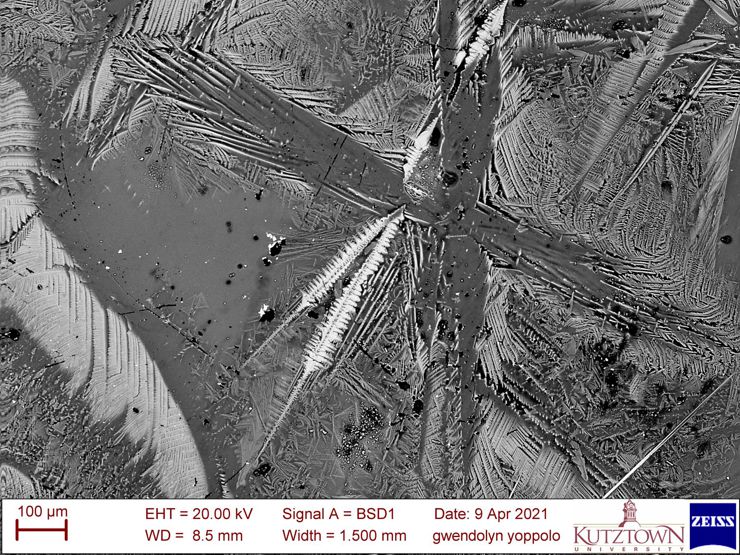
Backscatter Electron Detector (in chamber) = highlights differences between grains with different chemical compositions
Most of the electrons from the beam are absorbed into the sample, but some bounce back. Grains made of heavier elements bounce more electrons back up to the Backscatter Electron Detector and so appear brighter. The Backscatter Electron Detector is good for seeing compositional differences in the sample. This image of the branching microscopic crystals in a ceramic glaze was taken by professor gwendolyn yoppolo in Kutztown University's Art and Design Department using the Backscatter Electron Detector (BSD1).
-
In-lens Energy-Selective Backscatter Electron Detector = distinguishes chemical compositions for extremely small things (nanometer-scale)
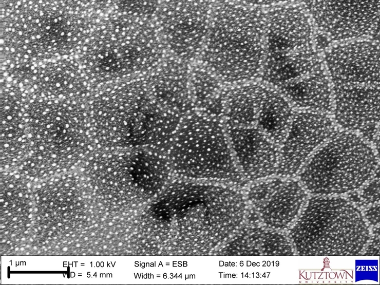
In-lens Energy-Selective Backscatter Electron Detector = distinguishes chemical compositions for extremely small things (nanometer-scale)
When the sample is very close to the pole piece, many of the backscatter electrons shoot up into the column. The In-lens Energy-Selective Backscatter Electron Detector (ESB) takes advantage of this to amplify the electron signal and image compositional differences of the sample. The device uses an electrified grid to deflect electrons the user wants to select out (that's the "energy-selective" part of the detector!) This image of tiny crystals grown on top of bigger crystals of a solar energy panel, taken by Kutztown University physics professor Dr. Justin Smoyer, used this detector.
-
Scanning Transmitted Electron Detector (STEM) = good for seeing organelles in cells and shapes of ultra-small grains
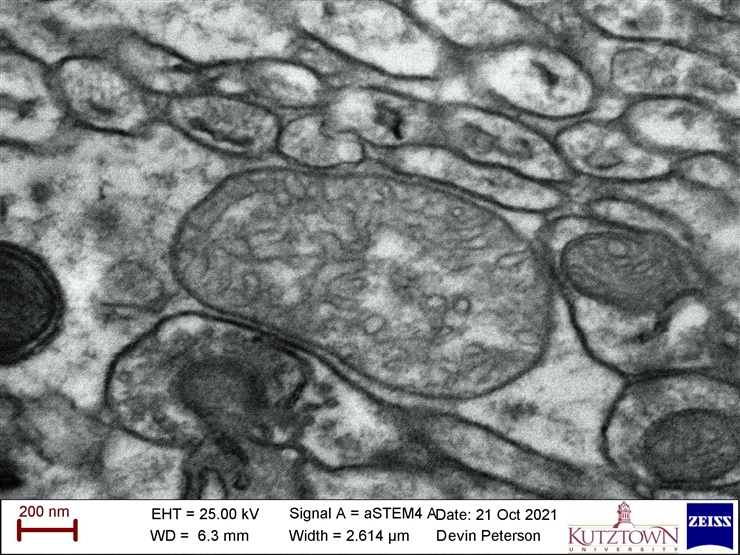
Scanning Transmitted Electron Detector (STEM) = good for seeing organelles in cells and shapes of ultra-small grains
Sometimes we want to see INSIDE a sample. We can shoot electrons straight through an ultra-thin slice of prepared cell tissue to create an image based on the electrons that get blocked by the sample, much like an x-ray image of bones in a body. This image of organelles in a mouse brain cell was taken by Devin Peterson – a student in the SEM course at Kutztown University – using the STEM detector.
Chemical analytical capabilities
In addition to being able to see the shapes of very tiny things, our SEM is equipped with an Oxford Ultim-Max 100mm2 Energy-dispersive X-ray Spectrometer (EDS) which analyzes the chemical composition of any point on the sample. The instrument can analyze a single one micrometer (0.00004 inch) spot, or do a complete chemical analysis of each individual pixel in an image to create a colorful map that documents broader chemical trends across the sample.
-
Chemical analyses of Individual Spots (1 micron)
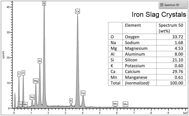
Spectrum for an individual spot chemical analyses using the EDS
When we focus the electron beam continuously on a single spot, the sample glows photons that are characteristic of the elements in the sample. The Energy-Dispersive X-ray Spectrometer (EDS) measures WHICH wavelengths of photons that glow from the sample, telling us which elements are present. The EDS also measures HOW MANY of each type of photon glow from the sample, from which we learn the concentrations. This graph is a spectrum of EDS data from a spot on a crystal in a sample of iron slag (an artificial lava created during the steel-making process). The y-axis reports how many x-rays glow (concentrations) for each wavelength (element) on the x-axis. We use these data to calculate the precise chemical composition of the sample.
-
Chemical composition map
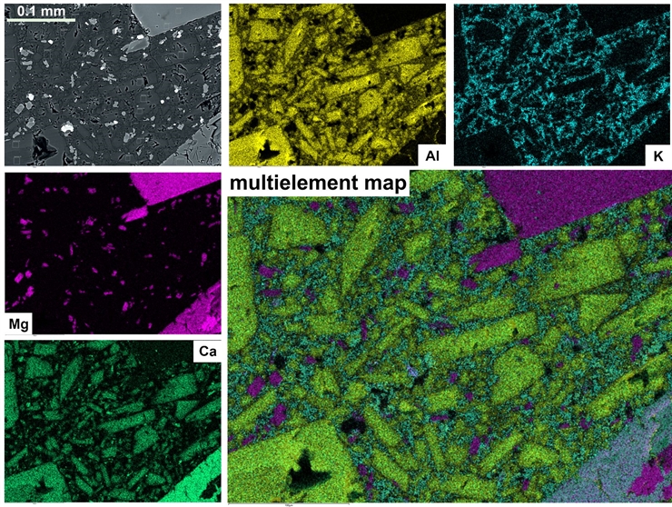
Chemical composition map
The electron beam is controlled by computer, so we can direct the SEM and EDS to analyze the chemical composition of each pixel in a picture. This is a remarkable capability because a typical image consists of 4,096 x 3,072 = 12,582,912 pixels, and the SEM/EDS can do these 12½ million analyses in about 10 minutes! There are two kinds of output for this tool: 1) map showing the distribution of each single specific element, and 2) map showing distribution of multiple elements. This composite image of a sample of volcanic rock from southern Colorado juxtaposes individual element maps (single color) and a composite multi-element map. The blocky green crystals contain calcium (Ca), aluminum (Al), and magnesium (Mg), but no potassium (K), so are the mineral augite pyroxene. The blocky purple crystals contain magnesium, but no calcium or aluminum, so are either enstatite pyroxene or olivine (the spectrum analysis can tell us which one). All of the potassium in the sample is in the space between the big, blocky crystals, which tells us potassium minerals formed last.